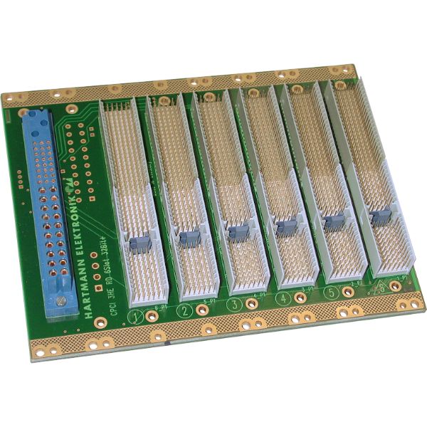
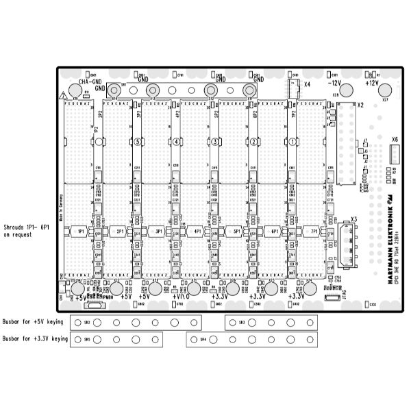
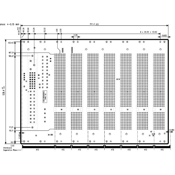
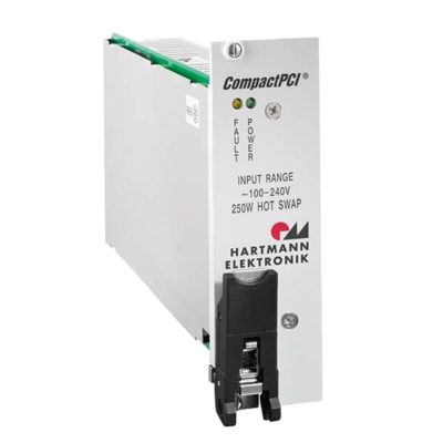
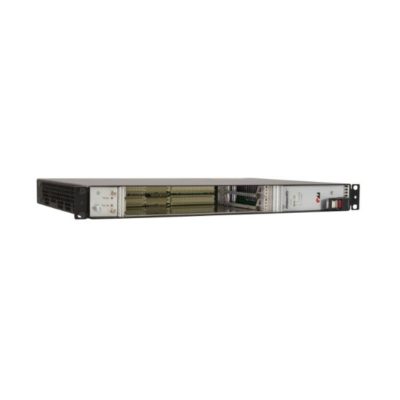
Hartmann Electronic’s board design is based on the HIGH-SPEED DESIGN concept. Low reflection is achieved by means of uniform signal surge impedance. The backplane design features an energy buffering feature which works across the entire frequency range. This guarantees improved reliability due to more stable supply voltages directly at each slot in conjunction with fluctuating loads. Continuous electrically conductive chassis GND surface located in the area where the backplane is mounted on the card rack. An M3 screw connection is available to connect chassis ground.
By installing a connecting bracket or busbar, chassis GND can be connected to ground in a low-resistance star arrangement. Separate 6-pin JTAG boundary scan connector is standard. Faster, simpler system initialization and testing via the JTAG bus when mounted in the chassis is achieved by direct access via an additional connector on the backplane
Main operating voltages are supplied via P 47 connector.

